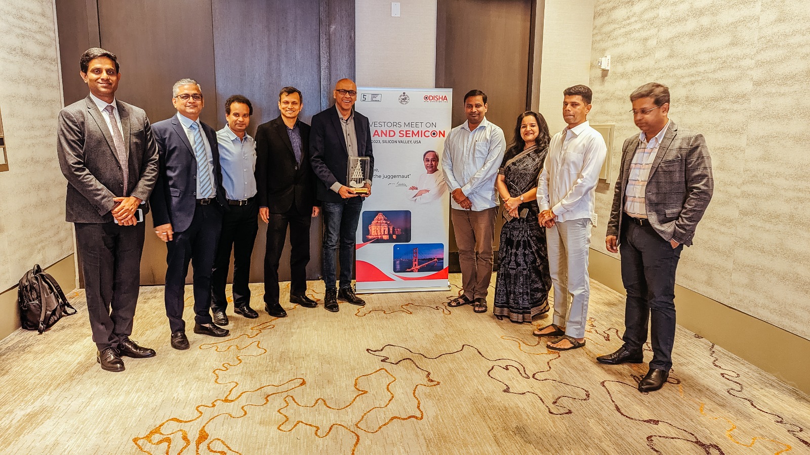
Palo Alto: On a day filled with noteworthy highlights, Synopsys, one of the global leaders in Electronics Design and Automation (EDA) with a presence in over 25 countries, announced its plans to set up a Bhubaneswar based design-centered facility. This facility, which will in phases expand to 300 chip design engineers performing high-tech roles, will comprise members from top Synopsys teams such as Hardware Analytics and Test (HAT) and Hardware Development Group(HDG), including HDG Analog and HDG Design/ Verification.
In a key meeting with the company, whose products include tools for logic synthesis and physical design of ICs, simulators for development, and debugging environments, the delegation interacted with Mr. Amit Sanghani, SVP, and Mr. Abhijeet Chakraborty, VP, and briefed them on the initiatives the Government is taking to build a resilient semiconductor ecosystem in the state.
The delegation highlighted how the state’s Semiconductor Manufacturing and Fabless Policy, which has received Cabinet approval, offers the most generous set of incentives to both fab and fabless units. It also provided details of the upcoming O-Chip program which will provide both design infrastructure and training support to researchers, startups, and companies.
Congratulating the delegation on the Government’s efforts, the Synopsys leadership pledged its earnest support to Odisha, and later, formally announced the company’s plan to set up a chip design centre in the state. The establishment of this centre will give a huge boost to Odisha’s semiconductor ambitions, strengthening the ecosystem and facilitating greater industry-readiness in the workforce.
To provide the best advisory and mentorship support for the O-Chip program, the delegation also held an extensive interaction with eminent industry leaders and researchers based in Silicon Valley. The O-Chip initiative, with a visionary goal to establish a next-generation Silicon Valley in Odisha, focuses on certain key objectives: empowering talent and industry expertise, facilitating internship and industry collaborations, forging research partnerships, fueling startup growth, and attracting semiconductor companies. With an initial focus on chips, embedded systems, and AI: Smart Labs, the program seeks collaboration with a diverse network of partners, including semiconductor companies, local and global universities, and a pool of industry experts.
The eminent industry leaders and researchers enthusiastically participated in the discussion which focused on the O-Chip initiative’s mode of operation, operational guidelines formulation, and advisory committee formation. They have generously offered to come onboard as advisors and mentors for the initiative. Their invaluable guidance and expertise will steer the initiative toward groundbreaking achievements, and lead to active participation of more semiconductor companies, universities, and industry experts.
The delegation also participated in an event with the Odia diaspora. Addressing the gathering, members of the delegation praised the diaspora for the manner in which it has preserved its socio-cultural ties with the homeland and the support it continues to provide for Odisha’s growth and prosperity. The event was organized by the Tourism Department in association with FICCI and witnessed participation of more than 900 people of Odisha origin. Consul General and the entire delegation hosted the Odia community.
The delegation’s visit to the Silicon Valley has been very successful with several global IT, electronics, semiconductor, and AI/ML companies having announced their plans to set up operations in the state. With Government push and support, Odisha is witnessing a great spurt in investment activity and creating more and more employment opportunities for its people.